|
SOLAR CELLS
|
||||||||||||||||||||||||
|
HOME | BIOLOGY | FILMS | GEOGRAPHY | HISTORY | INDEX | INVESTORS | MUSIC | SOLAR BOATS | SPORT |
||||||||||||||||||||||||
|
It's incredible that we've come this far. We can catch the Sun's radiant light energy and convert it into electrical energy. It's nothing new of course. Nature has been capturing the energy in light for millions of years. Each leaf is a form of solar cell, producing energy for plants and trees to grow in a chemical process known as Photosynthesis.
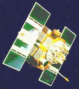
Solar panels power satellites
SPACE AGE TECHNOLOGY - Solar cells, also known as Photo Voltaic Cells, were rapidly developed to provide electrical energy for space missions. The beauty of solar cells is that provided the Sun shines, they keep on producing free electricity. Well, sort of free. Solar panels are still expensive to manufacture. It is the high purchase price and installation cost that effectively limits their use.
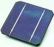
There are many types of solar cell. Polycrystaline (more than one crystal), monocrystaline and thin film. Monocrystaline is presently the most efficient at converting light energy into electricity. Sometimes as high as 20% but more usually 15%. A monocrystaline cell is made from a thin slice cut from a single crystal of silicon. A grid of metal is then embedded over the wafer ending in the contacts and other layers added. Thin film cells are plated onto a plate of glass. They are much cheaper to produce, but only around 5% efficient and heavy. Vehicle designers will normally want to capture as much energy as possible for a given area and weight.
A single cell is not of much practical use, producing less than a volt. Several cells have to be connected in a series of cells to produce a useable voltage. The voltage increases proportionally. 10 cells connected in series will produce about 7.5 volts. 20 cells 15 volts and so on. A number of cells (a battery) linked and mounted together is known as a solar panel.
HOW MUCH POWER - The Sun's energy reaching the surface of our planet is roughly 1 kilowatt per square meter. Before entering our atmosphere it is about 20% more: 1.2 kilowatts. That's why astronauts always look so bright. At 15% efficiency 10 panels each measuring 1meter by 1 meter would power 1 1/2 bars on an electric heater. 20 panels would power an electric kettle. This of course assumes that the sun is shining. Just imagine how many panels Solar Navigator needs to cross an ocean? Why not try and guess the area of panels on Solar Navigator.
"The
supply of solar energy is both without limit and cost;
Example of commercially available products:
Solar Solar Kits Solar Gadgets SOLAR CELL MANUFACTURERS WORLD WIDE
Essentially, solar panels are devices that convert light into electricity. They are called solar after the sun or "Sol" because the sun is the most powerful source of the light to use. They are sometimes called photovoltaics which means "light-electricity". Solar cells or PV cells rely on the photovoltaic effect to absorb the energy of the sun and cause current to flow between two oppositely charge layers.
Solar cell
Photovoltaics
Photovoltaic cells convert light energy into electricity at the atomic level. Although first discovered in 1839, the process of producing electric current in a solid material with the aid of sunlight wasn't truly understood for more than a hundred years. Throughout the second half of the 20th century, the science has been refined and the process has been more fully explained. As a result, the cost of these devices has put them into the mainstream of modern energy producers. This was caused in part by advances in the technology, where PV conversion efficiencies have improved considerably.
French physicist Edmond Becquerel first described the photovoltaic (PV) effect in 1839, but it remained a curiosity of science for the next three quarters of a century. At only 19, Becquerel found that certain materials would produce small amounts of electric current when exposed to light. The effect was first studied in solids, such as selenium, by Heinrich Hertz in the 1870s. Soon afterward, selenium PV cells were converting light to electricity at 1% to 2% efficiency. As a result, selenium was quickly adopted in the emerging field of photography for use in light-measuring devices.
Major steps toward commercializing PV were taken in the 1940s and early 1950s, when the Czochralski process was developed for producing highly pure crystalline silicon. In 1954, scientists at Bell Laboratories depended on the Czochralski process to develop the first crystalline silicon photovoltaic cell, which had an efficiency of 4%.
"What is often considered the first genuine solar cell was built around 1883 by Charles Fritts, who used junctions formed by coating selenium (a semiconductor) with an extremely thin layer of gold... These early solar cells, however, still had energy-conversion efficiencies of less than 1 percent. This impasse was finally overcome with the development of the silicon solar cell by Russell Ohl in 1941. Thirteen years later three other American researchers, G.L. Pearson, Daryl Chapin, and Calvin Fuller, demonstrated a silicon solar cell capable of a 6-percent energy-conversion efficiency when used in direct sunlight." - Encyclopedia Britannica
Solar Panels
A solar panel or battery converts the sun's energy to electricity. Gerald Pearson, Calvin Fuller and Daryl Chapin invented the first sun energy battery in 1954. The inventors created an array of several strips of silicon (each about the size of a razorblade), placed them in sunlight, captured the free electrons and turned them into electrical current. Bell Laboratories in New York announced the prototype manufacture of a new solar battery. Bell had funded the research. The first public service trial of the Bell Solar Battery began with a telephone carrier system (Americus, Georgia) on October 4 1955.
Sun Energy Battery - In 1954, G.L. Pearson, C.S. Fuller, and D.M. Chapin invented the first solar panel battery.
Solar panel array on Solar Navigator development model
Solar Panels in Space
When exposed to direct sunlight at 1 AU, a 6-centimeter diameter silicon cell can produce a current of about 0.5 ampere at 0.5 volt. Gallium arsenide is more efficient. Crystalline ingots are sliced into wafer-thin disks, polished to remove slicing damage, dopants are introduced into the wafers, and metallic conductors are deposited onto each surface: a thin grid on the sun-facing side and usually a flat sheet on the other. Spacecraft solar panels are constructed of these cells cut into appropriate shapes, protected from radiation and handling damage on the front surface by bonding on a cover glass, and cemented onto a substrate (either a rigid panel or a flexible blanket), and electrical connections are made in series-parallel to determine total output voltage. The cement and the substrate must be thermally conductive, because in flight the cells tend to heat up from absorbing infrared energy that is not converted to electricity. Since cell heating reduces the operating efficiency it is desirable to minimize the heating. The substrate is supported on a deployable structural framework. The resulting assemblies are called solar panels or solar arrays.
A solar panel is a collection of solar cells. Although each solar cell provides a relatively small amount of power, many solar cells spread over a large area can provide enough power to be useful. To get the most power, solar panels have to be pointed directly at the Sun. Spacecraft are built so that the solar panels can be pivoted as the spacecraft moves. Thus, they can always stay in the direct path of the light rays no matter how the spacecraft is pointed. Spacecraft are usually designed with solar panels that can always be pointed at the Sun, even as the rest of the body of the spacecraft moves around, much as a tank turret can be aimed independently of where the tank is going. A tracking mechanism is often incorporated into the solar arrays to keep the array pointed towards the sun.
Solar panels need to have a lot of surface area that can be pointed towards the Sun as the spacecraft moves. More exposed surface area means more electricity can be converted from light energy from the Sun. Sometimes, satellite scientists purposefully orient the solar panels to "off point," or out of direct alignment from the Sun. This happens if the batteries are completely charged and the amount of electricity needed is lower than the amount of electricity made. The extra power will just be vented by a shunt into space as heat.
Solar panels are very hardy. Compared to alternative power sources, they wear out very slowly. The principal factor affecting the loss in power with time is the Space radiation environment. For low radiation environments, such as low Earth orbiting, their effectiveness decreases around 1 to 2 percent a year. This means after a five year mission the solar panels will still be making more than 90% of what they made at the beginning of the mission (as long as they haven't gotten farther away from the Sun). In contrast, for missions in higher radiation environments, such as mid altitude Earth orbit (2000 to 10000 kilometers), arrays can lose half their power within 1 year. That is one reason few missions fly in this orbital range.
Photovoltaic concentrator solar arrays for primary spacecraft power are devices, which intensify the sunlight on the photovoltaics. This design uses lenses, called Fresnel* lenses, which take a large area of sunlight and direct it towards a specific spot by bending the rays of light and focusing them. Some people use the same principle when they use a magnifying lens to focus the Sun's rays on a pile of kindling or paper to start fires.
Solar concentrators put one of these lenses over every solar cell. This focuses light from the large concentrator area down to the smaller cell area. This allows the quantity of expensive solar cells to be reduced by the amount of concentration. Concentrators work best when there is a single source of light and the concentrator can be pointed right at it. This is ideal in space, where the Sun is a single light source. Solar cells are the most expensive part of solar arrays, and arrays are often a very expensive part of the spacecraft. This technology allows costs to be cut significantly due to the utilization of less material.
*Fresnel lenses have been around since Augustin Jean Fresnel invented them in 1822. Theaters use them for spotlights and lighthouses use them to make their lights visible at greater distances.
SOLAR CELL MANUFACTURERS WORLD WIDE A-Z
A solar, or photovoltaic cell, is a semiconductor device consisting of a large-area p-n junction diode, which, in the presence of sunlight is capable of generating usable electrical energy. This conversion is called the photovoltaic effect. The field of research related to solar cells is known as photovoltaics.
Solar cells have many applications. They are particularly well suited to, and historically used in situations where electrical power from the grid is unavailable, such as in remote area power systems, Earth orbiting satellites, handheld calculators, remote radiotelephones, water pumping applications, etc. Solar cells (in the form of modules or solar panels) are appearing on building roofs where they are connected through an inverter to the electricity grid in a net metering arrangement. The term "photovoltaic" comes from the Greek photos meaning light and the name of the Italian physicist Volta, after whom the volt (and consequently voltage) are named. It means literally of light and electricity.
INVENTOR MODERN SOLAR CELL
Russell Ohl is generally recognized for patenting the modern solar cell in 1946 US2402662, "Light sensitive device"). Sven Ason Berglund had a prior patent concerning methods of increasing the capacity of photosensitive cells.
Materials and efficiency
Various materials have been investigated for solar cells. There are two main criteria - efficiency and cost. Efficiency is a ratio of the electric power output to the light power input. Ideally, near the equator at noon on a clear day, the solar radiation is approximately 1000 W/m². So a 10% efficient module of 1 square meter can power a 100 W light bulb. Costs and efficiencies of the materials vary greatly. By far the most common material for solar cells (and all other semiconductor devices) is crystalline silicon. Crystalline silicon solar cells come in three primary categories:
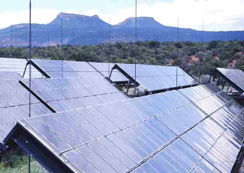
Sun powered solar tracking panel array
These technologies are wafer based manufacturing. In other words, in each of the above approaches, self supporting wafers of ~300 micrometres thick are fabricated and then soldered together to form a module. Thin film approaches are module based. The entire module substrate is coated with the desired layers and a laser scribe is then used to delineate individual cells. Two main thin film approaches are amorphous silicon and CIS:
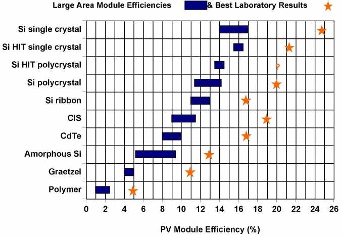
There are additional materials and approaches. For example, Sanyo has pioneered the HIT cell. In this technology, amorphous silicon films are deposited onto crystalline silicon wafers. The chart below illustrates the various commercial large area module efficiencies and the best laboratory efficiencies obtained for various materials and technologies. Interconnection and modules
Usually, solar cells are electrically connected, and combined into "modules", or solar panels. Solar panels have a sheet of glass on the front, and a resin encapsulation behind to keep the semiconductor wafers safe from the elements (rain, hail, etc). Solar cells are usually connected in series in modules, so that their voltages add.
THEORY
In order to understand how a solar cell works, a little background theory in semiconductor physics is required. For simplicity, the description here will be limited to describing the workings of single crystalline silicon solar cells.
Silicon is a group 14 (formerly, group IV) atom. This means that each Si atom has 4 valence electrons in its outer shell. Silicon atoms can covalently bond to other silicon atoms to form a solid. There are two basic types of solid silicon, amorphous (having no long range order) and crystalline (where the atoms are arranged in an ordered three dimensional array). There are various other terms for the crystalline structure of silicon; poly-crystalline, micro-crystalline, nano-crystalline etc, and these refer to the size of the crystal "grains" which make up the solid. Solar cells can be, and are made from each of these types of silicon, the most common being poly-crystalline.
Silicon is a semiconductor. This means that in solid silicon, there are certain bands of energies which the electrons are allowed to have, and other energies between these bands which are forbidden. These forbidden energies are called the "band gap". The allowed and forbidden bands of energy are explained by the theory of quantum mechanics.
At room temperature, pure silicon is a poor electrical conductor. In quantum mechanics, this is explained by the fact that the Fermi level lies in the forbidden band-gap. To make silicon a better conductor, it is "doped" with very small amounts of atoms from either group 13 (III) or group 15 (V) of the periodic table. These "dopant" atoms take the place of the silicon atoms in the crystal lattice, and bond with their neighbouring Si atoms in almost the same way as other Si atoms do. However, because group 13 atoms have only 3 valence electrons, and group 15 atoms have 5 valence electrons, there is either one too few, or one too many electrons to satisfy the four covalent bonds around each atom. Since these extra electrons, or lack of electrons (known as "holes") are not involved in the covalent bonds of the crystal lattice, they are free to move around within the solid. Silicon which is doped with group 13 atoms (aluminium, gallium) is known as p-type silicon because the majority charge carriers (holes) carry a positive charge, whilst silicon doped with group 15 atoms (phosphorus, arsenic) is known as n-type silicon because the majority charge carriers (electrons) are negative. It should be noted that both n-type and p-type silcion are electrically neutral, i.e. they have the same numbers of positive and negative charges, it is just that in n-type silicon, some of the negative charges are free to move around, while the converse is true for p-type silicon.
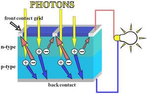
Photons absorb into electron-hole pairs, which diffuse to contacts
Light generation of carriers
When a photon of light hits a piece of silicon, one of two things can happen. The first is that the photon can pass straight through the silicon. This (generally) happens when the energy of the photon is lower than the bandgap energy of the silicon semiconductor. The second thing that can happen is that the photon is absorbed by the silicon. This (generally) happens if the photon energy is greater than the bandgap energy of silicon. When a photon is absorbed, its energy is given to an electron in the crystal lattice. Usually this electron is in the valence band, and is tightly bound in covalent bonds between neighbouring atoms, and hence unable to move far. The energy given to it by the photon "excites" it into the conduction band, where it is free to move around within the semiconductor. The covalent bond that the electron was previously a part of now has one less electron - this is known as a hole. The presence of a missing covalent bond allows the bonded electrons of neighboring atoms to move into the "hole," leaving another hole behind, and in this way a hole can move through the lattice. Thus, it can be said that photons absorbed in the semiconductor create mobile electron-hole pairs.
A photon only needs to have energy greater than the band gap energy to excite an electron from the valence band into the conduction band. However, the solar frequency spectrum approximates a black body spectrum at ~6000 K, and as such, much of the solar radiation reaching the Earth is composed of photons with energies greater than the band gap of silicon. These higher energy photons will be absorbed by the solar cell, but the difference in energy between these photons and the silicon band gap is converted into heat (via lattice vibrations - called phonons) rather than into usable electrical energy.
The p-n junction
A solar cell is a large-area semiconductor p-n junction. To understand the workings of a p-n junction it is convenient to imagine what happens when a piece of n-type silicon is brought into contact with a piece of p-type silicon. In practice, however, the p-n junctions of solar cells are not made in this way, but rather, usually, by diffusing an n-type dopant into one side of a p-type wafer.
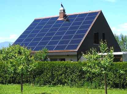
A truly solar powered house - zero carbon emissions
If we imagine what happens when a piece of p-type silicon is placed in intimate contact with a piece of n-type silicon, then what occurs is a diffusion of electrons from the region of high electron concentration - the n-type side of the junction, into the region of low electron concentration - p-type side of the junction. When the electrons diffuse across the p-n junction, they recombine with holes on the p-type side. This diffusion of carriers does not happen indefinitely however, because of the electric field which is created by the imbalance of charge immediately either side of the junction which this diffusion creates. Electrons from donor atoms on the n-type side of the junction are crossing into the p-type side, leaving behind the (extra) positively charged nuclei of the group 15 donor atoms, leaving an excess of positive charge on the n-type side of the junction. At the same time, these electrons are filling in holes on the p-type side of the junction, becoming involved in covalent bonds around the group 13 acceptor atoms, making an excess of negative charge on the p-type side of the junction. This imbalance of charge across the p-n junction sets up an electric field which opposes further diffusion of charge carriers across the junction.
This region where electrons have diffused across the junction is called the depletion region because it no longer contains any mobile charge carriers. It is also known as the "space charge region".
The electric field which is set up across the p-n junction creates a diode, allowing current to flow in only one direction across the junction. Electrons may pass from the n-type side into the p-type side, and holes may pass from the p-type side to the n-type side. But since the sign of the charge on electrons and holes is opposite, conventional current may only flow in one direction.
Separation of carriers by the p-n junction
Once the electron-hole pair has been created by the absorption of a photon, the electron and hole are both free to move off independently within the silicon latttice. If they are created within a minority carrier diffusion length of the junction, then, depending on which side of the junction the electron-hole pair is created, the electric field at the junction will either sweep the electron to the n-type side, or the hole to the p-type side.
Connection to an external load
If Ohmic metal-semiconductor contacts are made to both the n-type and p-type sides of the solar cell, and the electrodes connected to an external load, then electrons which are created on the n-type side, or have been "collected" by the junction and swept onto the n-type side may travel through the wire, power the load, and continue through the wire until they reach the p-type semiconductor-metal contact where they recombine with a hole which was either created as an electron-hole pair on the p-type side of the solar cell, or swept across the junction from the n-type side after being created there.
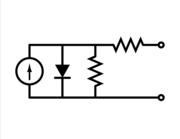
Equivalent circuit of a solar cell
To understand the electronic behaviour of a solar cell, it is useful to create a model which is electrically equivalent, and is based on discrete electrical components whose behaviour is well known. An ideal solar cell may be modelled by a current source in parallel with a diode. In practice no solar cell is ideal, so a shunt resistance and a series resistance component are added to the model. The result is the "equivalent circuit of a solar cell" shown on the left. Also shown on the right, is the schematic representation of a solar cell for use in circuit diagrams.
Manufacture and devices
Because solar cells are semiconductor devices, they share many of the same processing and manufacturing techniques as other semiconductor devices such as computer and memory chips. However, the stringent requirements for cleanliness and quality control of semiconductor fabrication are a little more relaxed for solar cells.
Most large-scale commercial solar cell factories today make screen printed poly-crystalline silicon solar cells. Single crystalline wafers which are used in the semiconductor industry can be made in to excellent high efficiency solar cells, but they are generally considered to be too expensive for large-scale mass production.
Poly-crystalline silicon wafers are made by wire-sawing block-cast silicon ingots into very thin (250 to 350 micrometre) slices or wafers. The wafers are usually lightly p-type doped. To make a solar cell from the wafer, an n-type diffusion is performed on the front side of the wafer, forming a p-n junction a few hundred nanometres below the surface.
Antireflection coatings, which increase the amount of light coupled into the solar cell, are typically applied next. Over the past decade, silicon nitride has gradually replaced titanium dioxide as the antireflection coating of choice because of its excellent surface passivation qualities (i.e., it prevents carrier recombination at the surface of the solar cell). It is typically applied in a layer several hundred nanometers thick using plasma-enhanced chemical vapor deposition (PECVD).
The wafer is then metallised, whereby a full area metal contact is made on the back surface, and a grid-like metal contact made up of fine "fingers" and larger "busbars" is screen-printed onto the front surface using a silver paste. The rear contact is also formed by screen-printing a metal paste, typically aluminum. Usually this contact covers the entire rear side of the cell, though in some cell designs it is printed in a grid pattern. The metal electrodes will then require some kind of heat treatment or "sintering" to make Ohmic contact with the silicon.
After the metal contacts are made, the solar cells are interconnected in series (and/or parallel) by flat wires or metal ribbons, and assembled into modules or "solar panels". Solar panels have a sheet of tempered glass on the front, and a polymer encapsulation on the back.
Some solar cells have textured front surfaces that, like antireflection coatings, serve to increase the amount of light coupled into the cell. Such surfaces can usually only be formed on single-crystal silicon, though in recent years methods of forming them on multicrystalline silicon have been developed.
|
||||||||||||||||||||||||


| 1 | 2 | 3 |
| 4 | 5 | 6 |
|
|
|||
LINKS
Use of solar cells in Kenya and Uganda, in Africa
Pennicott, Katie, "Solar cell edges towards endless energy". 7 December 2001.
Dye Sensitized Solar Cells (DYSC) based on Nanocrystalline Oxide Semiconductor Films
News searching: Solar Cell, Photovoltaic
Historical: Photovoltaic Solar Energy Conversion: An Update
Wladek Walukiewicz, Materials Sciences Division, Berkeley Lab.: Full Solar Spectrum Photovoltaic Materials Identified. Quote: "... Maximum, theoretically predicted efficiencies increase to 50%, 56%, and 72% for stacks of 2, 3, and 36 junctions with appropriately optimized energy gaps, respectively...."
CNET: 5/12/03 SunPower Announces World's Most Efficient, Low-Cost Silicon Solar Cell Quote: "...The National Renewable Energy Laboratory (NREL) has verified 20.4 percent conversion efficiency for the A-300...."
SunPower A-300 (pdf), SunPower
29 March 2002, Scientists Create New Solar Cell Quote: "...semiconducting plastic material known as P3HT... 1.7 percent for sunlight..."
15 February 03, 'Denim' solar panels to clothe future buildings Quote: "... Unlike conventional solar cells, the new, cheap material has no rigid silicon base..."
Residential Solar Power Systems - Photo Gallery
Examples of Photovoltaic Systems
azonano.com: Carbon Nanotube Structures Could Provide More Efficient Solar Power for Soldiers 28 February 2005
![]()
Healthier alternative tastes for adventure capitalists

This
website
is Copyright © 1999 & 2008 NJK. The bird ![]() logo and name Solar Navigator and Solar Cola are trademarks. All
rights reserved. All other trademarks are hereby acknowledged. Max
Energy Limited is
an educational charity.
logo and name Solar Navigator and Solar Cola are trademarks. All
rights reserved. All other trademarks are hereby acknowledged. Max
Energy Limited is
an educational charity.
AUTOMOTIVE | BLUEBIRD | ELECTRIC CARS | ELECTRIC CYCLES | SOLAR CARS